
The manufacturer website of HQ Graphene's popular product "Transfer Stage" has been renewed.The high-quality transcription system has also been updated, so we will introduce new features.
More information can be found on the official website of HQ Graphene Systems BV:
https://www.hq2d.com/
At our company, HQ Graphene's "High Quality 2D Transfer Systems (formerly known as 2D Heterostructure Transfer Systems)” is handled.
At this time (August 2023), the lineup includes a fully automatic transfer system, a manual system, and a partially electric system.Manufacturers can also design custom systems for special requirements, such as nanowire manipulation equipment or HQ Graphene, Inc., for nanowire manipulation equipment.
If you have any questions about product details or custom orders, please feel free to contact us.
HQ GrapheneAbout the company
![]()
![]()
A Dutch nanotechnology company based on the University of Groningen campus.We specialize in the production and characterization of hexagonal boron nitride, single crystal graphene, various sulfides (MoS2, WS2, TiS2, etc.), selenides (GaSe, NbSe2, etc.), and tellurides (Bi2Te3, MoTe2, etc.). HQ Graphene supplies these high-purity, high-quality crystals to over 190 universities, research institutes and companies around the world to support the advancement of scientific research.

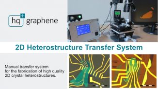
High Quality 2D Transfer Systems
HQ Graphene's 2D Transfer Systems are all-inclusive systems for the production of high-end 2D heterostructures and twisted bilayer graphene (twisted graphene).
The main part of the system is a manual rotary stage with a precision 0.015 degree resolution.This allows the material to be precisely positioned at the required angle.A high-resolution optical microscope (with selectable brightfield/darkfield illumination) and a CCD camera are also included for visual inspection and alignment.
The substrate is fixed in a vacuum and can be controlled from room temperature to a maximum of 200°C with an accuracy of 0.1°C.This allows the required temperature to be optimally maintained during the bonding process.
The compact design also allows the system to be easily installed in a glovebox and to handle air-sensitive materials.
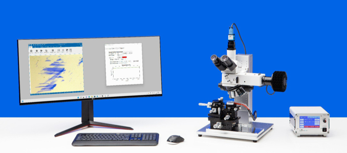
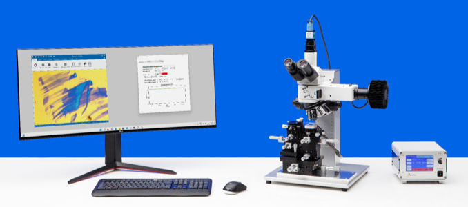
System configuration
- Optical microscope (long-distance objective lens and long working objective lens)
- CCD camera (measurement function for distance, angle, etc.)
- monitor
- Tilt rotary stage
- Vacuum chuck (heating and cooling function)
- controller for control
Type of transfer system
A high-quality 2D transfer system for fabricating heterostructures and twisted bilayers.
Designed for precise placement of stamps (hexagonal boron nitride, graphene, etc.) on a substrate, allowing them to be moved relative to each other not only in the X, Y and Z directions, but also by tilt and rotation .This maximizes the degree of freedom in arranging the 2D crystal flakes.
Currently, we have a lineup of fully automatic transfer systems, manual systems, and partially electric systems, and it is possible to consult about selection and arbitrary specifications according to your needs.
Fully motorized transfer system (HQ2D MOT)

A fully automatic transfer system in which software completely controls transfer operations other than loading samples (materials) and masks.Ideal for glovebox use for handling sensitive materials.Intuitive operation guides you through each procedure, and it has convenient functions such as saving images and storing sample positions.
Manual transfer system (HQ2D MAN)
A compact manual transfer system for users who prefer manual work.Fine adjustment is possible with a micromanipulator, and heating, cooling, and vacuum control are integrated and can be operated with a touch screen.
Customized transfer systems (HQ2D MOD)
A modified transfer system with XY and Z stages placed under the sample and mask.There are models that can manipulate nanowires, models that have orientable needles inside, and models that have pure brightfield only microscopes.Please confirm the desired configuration and specifications.
We have a track record of handling materials for nanoelectronics, quantum computing, new material research, etc.
If you have any questions, please feel free to contact us.
| Click here for product details and inquiries
High Quality 2D Transfer System / 2D heterostructure fabrication system by transfer Maker (HQ Graphene BV/ HQ Graphene Systems BV ) website
|